SK Hynix Begins Construction of Next-Generation Semiconductor Production Base in Indiana, USA
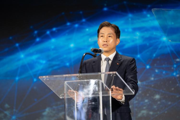
SK Hynix held a groundbreaking ceremony for the construction of a production base for High Bandwidth Memory (HBM), a core component of artificial intelligence (AI) semiconductors, in Indiana, USA. This project is considered a significant step toward strengthening technological cooperation between South Korea and the United States and enhancing competitiveness in the global AI semiconductor market.
The new Indiana plant is slated to be used as an advanced packaging facility for HBM production. Through this plant, SK Hynix plans to respond to the rapidly increasing global demand for AI semiconductors and further expand its cooperation with major big tech companies in the U.S.
Officials who attended the groundbreaking ceremony emphasized that this investment would be a great boon to the economic and technological development of both South Korea and the U.S. In particular, Indiana is emerging as a new hub for the semiconductor industry, and it is expected to have a positive impact on regional economic revitalization and job creation.
Through this U.S. investment, SK Hynix intends to stabilize its global supply chain and further accelerate the development of next-generation semiconductor technology. Efforts by South Korean companies to secure leadership in the AI semiconductor sector in the global market are continuing.